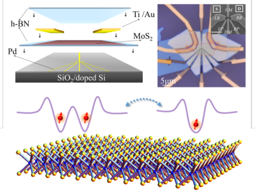
The Key Laboratory of Quantum Information of the Chinese Academy of Sciences, led by Guo Guangcan, a member of the Chinese Academy of Sciences and a professor at the University of Science and Technology of China, made progress in the research of semiconductor-gated quantum dots. The research team Guo Guoping and his collaborators explored the possibility of applying two-dimensional layered transition metal chalcogenide to semiconductor quantum chips. For the first time, quantum-point devices with full electrical control were realized in the semiconductor flexible two-dimensional material system. . The results were published online October 20 in Science Advances.
After decades of development, semiconductor-gated quantum dots as a quantum transistor have become one of the popular candidate systems for quantum chips. The two-dimensional material system represented by graphene has become one of the key research objects of flexible electronics and quantum electronics due to its natural monoatomic layer thickness, excellent electrical properties and easy integration. However, in the more than ten years since the discovery of graphene, scientists have tried a lot of experiments and found that the band structure and interface defect impurities in graphene have a great influence on the performance of quantum dot devices. At present, quantum dots in two-dimensional materials cannot achieve effective electrical regulation.
Based on this, Guo Guoping's research group and its collaborators selected the new two-dimensional material molybdenum disulfide for in-depth research. The material has a suitable band gap, strong spin-orbit coupling strength and rich spin-energy-related physical phenomena, and has broad applications in quantum electronics, especially spintronics and energy valley electronics. prospect. After a lot of attempts, the researchers used a series of modern semiconductor processes such as micro-nano processing and low-temperature LED irradiation to combine the boron nitride encapsulation technology widely used in the current two-dimensional material system research to effectively reduce impurities in the quantum dot structure. Defects, etc., for the first time, an all-electrically controllable double quantum dot structure was realized in such materials. At very low temperatures, a single quantum dot of about 128 nm can be modulated into two single-quantity double quantum dot systems with a size of about 68 nm by electrode voltage. The inter-point electron tunneling of a double quantum dot system can be passed. Monotonic regulation of the electrode voltage enables electrical controllable modulation of artificial atoms to man-made molecules. This controllable single-electron tunneling device provides a possible platform for studying the physical phenomena associated with the spin and energy valley degrees of the material at a single electron level. Using this platform, the researchers observed that the device conductance decreased as the external magnetic field increased. This phenomenon, known as Coulomb blocking and anti-localization, reveals the effects of short-range defects and spin-orbit coupling on the electrical transport properties in molybdenum disulfide.
The research work was supported by the National Fund Committee, the Ministry of Science and Technology, the Chinese Academy of Sciences, and the Center for Collaborative Innovation of Quantum Information and Quantum Technology. Some of the sample processing procedures in the experiment were completed at the China University of Science and Technology Micro-Nano Research and Manufacturing Center.

Glued Laminated Timber(Glulam), known in Japan as integrated material, is a commonly used wood structure construction material that can be made into large-span curved beams and is widely used in the manufacture of large public places. The advantages of the glulam prefabricated home:
High Quality Material:The glulam prefabricated home has been built millions of times in North America. They are strong, warm, durable, energy-efficient, renewable, etc. Used for Vacation House ,Residential House, Resort Hotels , Glulam Homes and Commercial Houses.
Vacation House,Residential house,Resort Hotels,Glulam Homes, Commercial Houses
Dalian Quacent New Building Materials Co.,Ltd. , https://www.quacenthomes.com